
Designing a printed circuit board is one of the most important stages in turning an electronic idea into a real product. A schematic may look correct, components may appear properly connected, and the PCB may even pass basic design-rule checks — but that does not guarantee the first prototype will work correctly.
Small PCB design mistakes can cause serious problems such as unstable power, communication failures, excessive noise, overheating, unreliable wireless performance, manufacturing difficulties, or even permanent component damage.
The good news is that many of these problems can be prevented before manufacturing.
In this guide, we will look at 10 common PCB design mistakes, why they happen, how they affect a prototype, and what designers can do to avoid them.

1. Poor Component Placement
Component placement is one of the foundations of good PCB design.
A common mistake is placing components primarily based on where they fit rather than considering how they electrically interact.
Poor placement can result in:
- Long signal traces
- Difficult routing
- Larger current loops
- Increased electrical noise
- Poor thermal performance
- Difficult assembly
- Reduced wireless performance
Before routing begins, components should be grouped according to their function.
For example:
- Power components should remain close to the power-input section.
- Decoupling capacitors should be close to IC power pins.
- Crystal components should be close to the microcontroller.
- RF components should remain close to the antenna or RF section.
- Sensor components may need separation from heat-generating devices.
A well-planned component placement can make routing significantly easier and improve overall reliability.
Start With Functional Blocks
One useful approach is to divide the board into functional areas such as:
Power Input → Power Regulation → Microcontroller → Sensors → Communication → Outputs
This helps create a logical physical layout before traces are routed.
Good PCB layout starts with placement, not routing.
2. Incorrect Decoupling Capacitor Placement
Decoupling capacitors are small components with a very important job.
They help provide local energy during rapid changes in current demand and help reduce unwanted noise on power rails.
A common PCB mistake is placing the correct capacitor value but locating the capacitor too far from the IC power pin.
For example, a schematic may correctly include a 100 nF capacitor between VCC and GND. However, if that capacitor is placed far away from the microcontroller on the PCB, its effectiveness at high frequencies can be reduced.
The capacitor should generally be located close to the relevant supply pin with short connections to power and ground.
Why Decoupling Matters
Modern microcontrollers and digital ICs can switch very quickly.
During switching, they may require short bursts of current.
Without effective local decoupling, problems may include:
- Unexpected resets
- ADC noise
- Communication errors
- Unstable sensors
- Random firmware behavior
- EMI problems
For complex ICs, designers should carefully follow the manufacturer's recommended decoupling arrangement.
The datasheet and hardware design guidelines should always be checked.
3. Using Traces That Are Too Thin for the Current
Not every PCB trace should have the same width.
A signal trace carrying a few milliamps has very different requirements from a trace carrying several amperes to a motor, pump, heater, LED array, or power converter.
Using traces that are too narrow can lead to:
- Excessive voltage drop
- Heating
- Reduced efficiency
- Unstable loads
- Damaged traces in severe cases
High-current paths should be identified before routing.
Examples may include:
- Battery input
- Motor supply
- Pump supply
- Relay contacts
- High-power LEDs
- DC-DC converter paths
- USB power
- Ground return paths
Trace Width Depends on More Than Current
Required trace width can depend on:
- Current
- Copper thickness (e.g. 1 oz vs 2 oz)
- Trace length
- External or internal PCB layer
- Acceptable temperature rise
- Allowed voltage drop
- Ambient temperature
Instead of guessing, use appropriate PCB current/temperature calculations and applicable design standards (such as IPC-2152) or manufacturer guidance.
For high-current designs, copper pours or dedicated planes may be more appropriate than narrow traces.
4. Poor Grounding and Ground Return Paths
Ground is not simply a collection of points that can be connected anywhere without considering current flow.
Current travels in loops.
A signal travels from its source to its destination and requires a return path.
Poor return paths can contribute to:
- EMI (Electromagnetic Interference)
- Signal integrity problems
- ADC instability
- Sensor noise
- Communication errors
- Unpredictable behavior
A continuous ground plane is often beneficial in many digital and mixed-signal PCB designs (see our complete PCB design guide).
Avoid Unnecessary Ground-Plane Interruptions
Routing traces or creating large gaps in a ground plane can force return currents to travel around obstacles.
This increases loop area and can degrade signal integrity.
Designers should consider not only where the signal trace goes but also how its return current flows.
High-Current Ground Paths
High-current loads such as motors, pumps, relays, and power converters can generate electrical noise.
Sensitive analog sensors should not unintentionally share problematic return paths with noisy loads.
Grounding strategy should be based on the actual circuit architecture rather than blindly separating every ground into different regions.
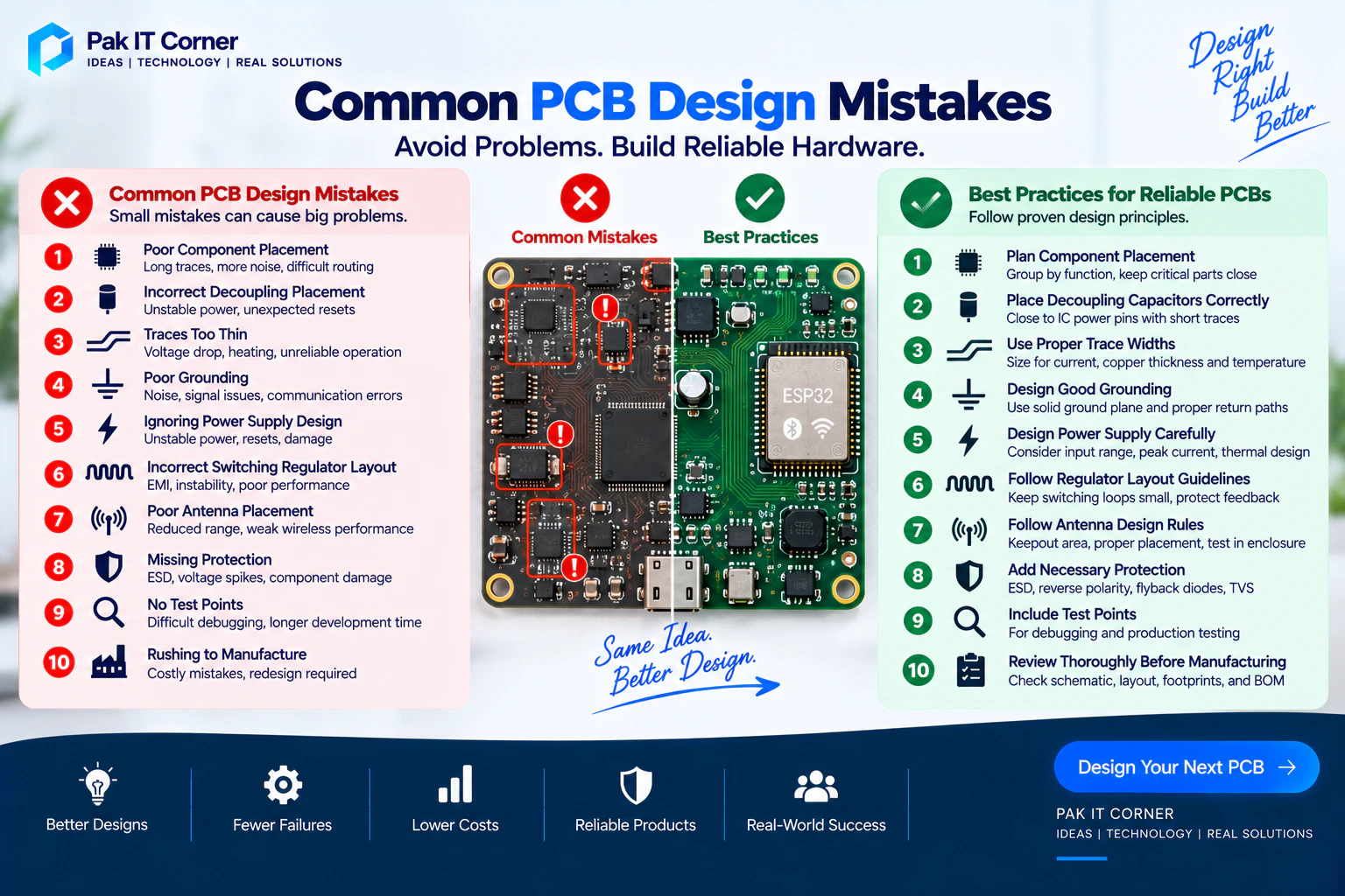
5. Ignoring Power Supply Design
A PCB can have a perfectly programmed microcontroller and still fail because its power system was not designed properly.
Power design is one of the most common sources of prototype problems.
Important questions include:
- What is the input voltage range?
- What is the maximum load current?
- What happens during startup?
- What happens when a motor starts?
- What is the peak current required by the wireless module?
- How much voltage drop occurs?
- How much heat will the regulator generate?
- Are the input and output capacitors appropriate?
- Is reverse-polarity protection needed?
Regulator Selection
Suppose a board receives 12 V and requires 3.3 V.
Using a linear regulator may appear simple, but significant power can be dissipated as heat depending on load current.
Power dissipation for a linear regulator can be approximated as:
P = (Vin − Vout) × I
For higher voltage differences or higher currents, a switching regulator may be more appropriate.
However, switching converters also require careful component selection and PCB layout.
Peak Current Matters
Wireless modules such as Wi-Fi (ESP32), cellular, GNSS-related systems, and other radios can have changing current demands.
Designing only around average current can cause voltage dips and unexpected resets.
Always consider worst-case and transient requirements.
6. Incorrect Switching Regulator Layout
A switching regulator can work perfectly on a manufacturer's evaluation board but perform poorly on a custom PCB if the layout is incorrect.
This is because switching power supplies contain fast-changing currents.
Critical components may include:
- Input capacitor
- Output capacitor
- Inductor
- Switching MOSFETs
- Diode, where applicable
- Feedback network
These components should be placed according to the regulator manufacturer's recommended layout.
Keep Switching Loops Small
High-current switching loops should generally be kept compact.
Long traces in these areas can increase:
- Noise
- EMI
- Voltage spikes
- Ringing
- Instability
The switch node is particularly important.
It should not be unnecessarily large or routed close to sensitive analog signals.
Feedback Routing
Feedback signals should be protected from noisy switching nodes.
Poor feedback routing can result in unstable or inaccurate output voltage.
When designing with a buck, boost, or buck-boost converter, the datasheet's reference PCB layout is extremely valuable.
7. Poor Antenna Placement
Wireless products introduce another major PCB design challenge: antenna performance (see our BLE vs Wi-Fi IoT guide).
A perfectly functioning ESP32, Bluetooth, Wi-Fi, LoRa, GNSS, or other wireless circuit can still have poor range if the antenna environment is badly designed.
Common antenna-layout mistakes include:
- Copper underneath an antenna keepout area
- Ground plane where the module requires clearance
- Components too close to the antenna
- Battery directly behind the antenna
- Metal enclosure blocking the antenna
- Antenna located between noisy components
- Poor board-edge placement
Module Antennas
Many wireless modules include integrated PCB antennas.
For example, an ESP32 module with an onboard antenna may require a specific keepout region.
The module manufacturer's hardware design guidelines should be followed carefully.
External Antennas
Products using external antennas require proper RF routing and connector placement.
RF traces may require controlled impedance and should generally be kept short and routed according to the relevant RF design requirements.
Antenna performance should be tested in the final enclosure because the enclosure, battery, cables, and nearby materials can change RF behavior.
8. Forgetting Protection Components
A prototype is often connected to cables, batteries, USB ports, motors, relays, and external sensors.
These connections expose the PCB to electrical conditions that may not occur during ideal bench testing.
Protection may be required against:
- Reverse polarity
- ESD (Electrostatic Discharge)
- Voltage spikes
- Overcurrent
- Inductive kickback
- Input transients
Flyback Protection
When switching an inductive load such as a relay, solenoid, or DC motor, stored energy in the load can produce a voltage spike when current is interrupted.
Appropriate suppression — often involving a flyback diode for suitable DC inductive loads — can protect the switching device and surrounding electronics.
The exact suppression method depends on the application.
USB and External Connectors
External connectors can be exposed to electrostatic discharge.
Appropriate ESD protection may be required for:
- USB ports
- Buttons exposed to users
- External sensor connectors
- Communication ports
- Other accessible interfaces
Protection should be selected according to the electrical characteristics of the interface.
9. Not Adding Test Points and Programming Access
A PCB may look cleaner without extra test pads, but debugging becomes much more difficult when the first prototype arrives.
Useful test points may include:
- Main input voltage
- 5 V rail
- 3.3 V rail
- Ground
- Reset
- Boot
- UART TX/RX
- I2C SDA/SCL
- SPI signals
- Important analog signals
Programming and debugging interfaces should also be accessible.
Depending on the microcontroller, this might include:
- UART
- SWD
- JTAG
- USB
- ICSP
- Dedicated programming pads
Think About Production Testing Early
Test points are not only useful during development.
They can also support production fixtures used to verify assembled boards.
A production test fixture may check:
- Power rails
- MCU communication
- Sensors
- LEDs
- Buttons
- Wireless communication
- Outputs
- Programming
Design for Testability (DFT) should ideally be considered before mass production.
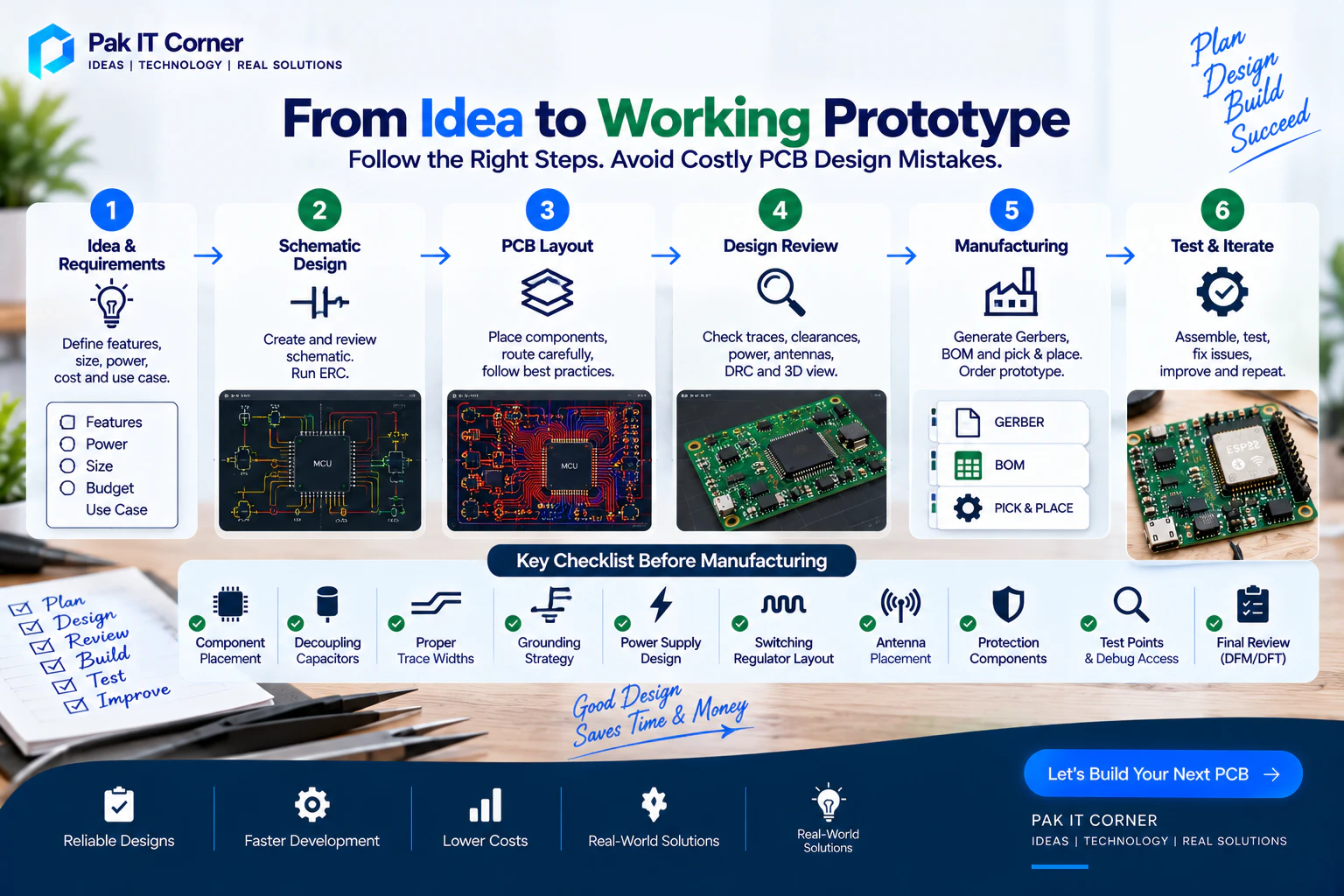
10. Sending the PCB to Manufacturing Without a Final Review
One of the most expensive PCB mistakes is rushing to fabrication.
A designer finishes routing, sees zero DRC errors, and immediately generates Gerber files.
But DRC cannot identify every possible design problem.
Before manufacturing, perform a systematic final review.
Check the Schematic
Verify:
- Power pins
- Ground pins
- Component values
- Part numbers
- Pin assignments
- Pull-up and pull-down resistors
- Programming interfaces
- Connector pinouts
- Protection components
- Power sequencing where relevant
Check the PCB
Verify:
- Component orientation
- Pin 1 markings
- Diode polarity
- LED polarity
- Electrolytic capacitor polarity
- Connector orientation
- Mounting holes
- Board dimensions
- Antenna clearance
- Trace widths
- Power paths
- Ground plane
- Silkscreen
- Test points
Check the Footprints
Footprint errors can completely ruin an otherwise correct PCB.
Always verify critical footprints against the manufacturer's mechanical drawings.
Pay special attention to:
- IC packages
- Connectors
- USB-C connectors
- Switches
- Relays
- Modules
- MOSFETs
- Diodes
- Specialized sensors
Do not rely only on a library name.
Review the 3D Model
A 3D PCB view can help detect mechanical issues such as:
- Connectors facing the wrong direction
- Components interfering with the enclosure
- Incorrect component height
- Mounting-hole problems
- Overlapping components
However, a 3D model does not replace checking the actual footprint dimensions.
Bonus Mistake: Ignoring Component Availability
A technically perfect PCB cannot be manufactured if critical components are unavailable.
Before finalizing the design, check:
- Manufacturer part number
- Distributor availability
- Package
- Lifecycle status
- Lead time
- Alternative components
- Minimum order quantities
For prototypes, sourcing may appear easy because only a few parts are required.
Production is different.
A component that becomes unavailable can force a PCB redesign.
Where appropriate, consider second-source or alternative components during the design phase.
Bonus Mistake: Choosing the Wrong Component Package
A component may exist in several package options.
For example, the same IC family might be available as:
- QFN
- TQFP
- BGA
- SOIC
- SOT-23
- WLCSP
The smallest package is not always the best choice.
Package selection can affect:
- Assembly cost
- Hand solderability
- Inspection
- Thermal performance
- PCB routing
- Manufacturing yield
Prototype and production requirements should both be considered.
Bonus Mistake: Ignoring Thermal Design
Components that dissipate significant power require appropriate thermal consideration.
Potential heat sources include:
- Voltage regulators
- MOSFETs
- Motor drivers
- Charging ICs
- High-power LEDs
- Processors
- Wireless modules
- Power resistors
Thermal management may involve:
- Copper area
- Thermal vias
- Appropriate package selection
- Component spacing
- Heatsinking
- Airflow
- Enclosure design
A circuit that works for two minutes on a bench may behave differently after operating continuously inside a sealed enclosure.
Bonus Mistake: Ignoring Mechanical Requirements
Electronics do not operate in isolation.
The PCB eventually needs to fit inside a physical product.
Before finalizing the PCB, confirm:
- Board dimensions
- Mounting-hole positions
- Connector positions
- Button alignment
- LED locations
- Display position
- Antenna clearance
- Cable access
- Battery location
- Enclosure height
- Screw clearance
Mechanical constraints should ideally be defined before PCB layout begins.
PCB Design Checklist Before Manufacturing
Before ordering your prototype PCB, review at least the following areas systematically:
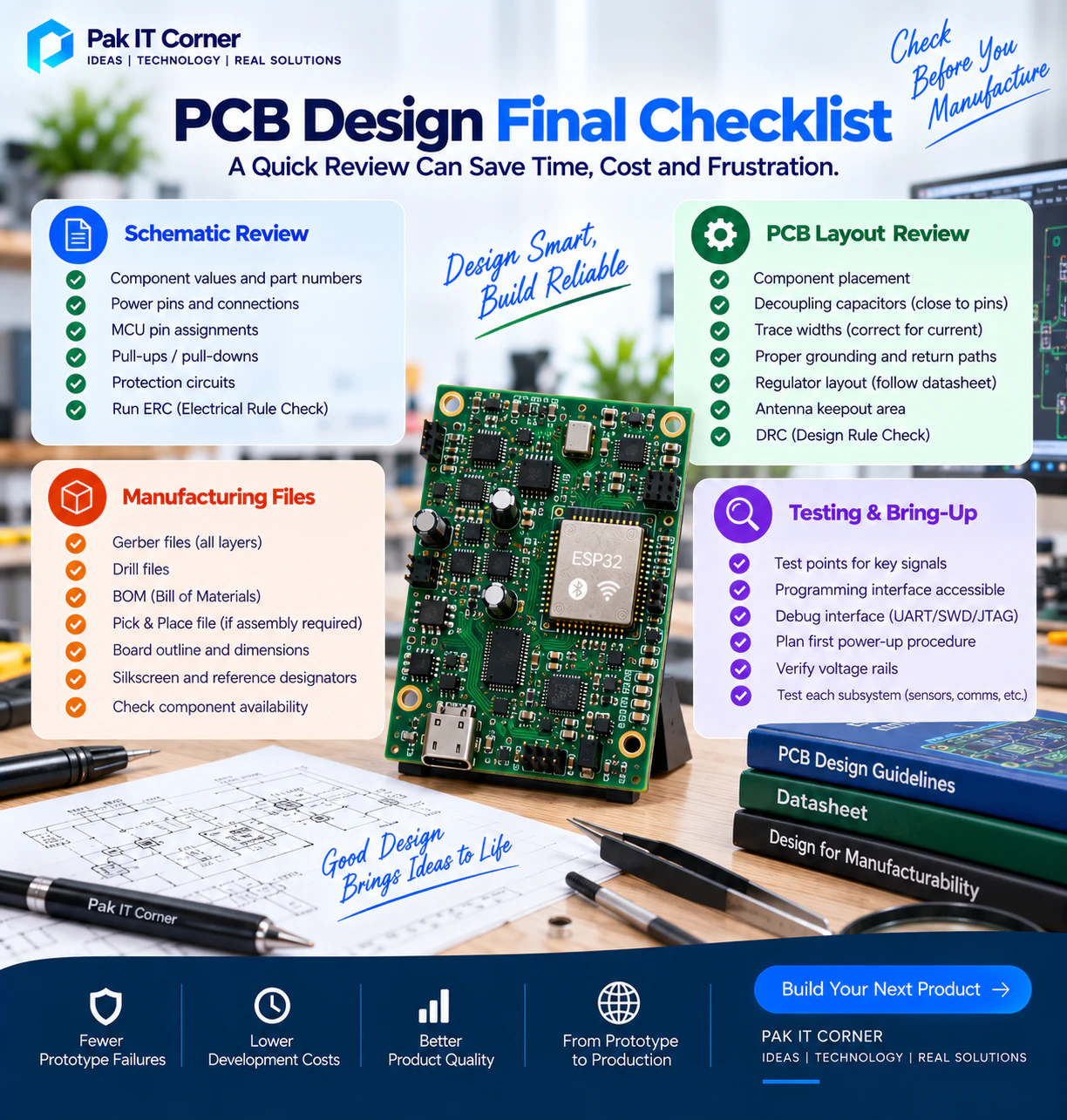
Schematic
- Power connections verified
- Component values checked
- MCU pins verified
- Communication buses checked
- Connector pinouts confirmed
- Pull-ups/pull-downs included where required
- Protection reviewed
- ERC completed
PCB Layout
- Component placement reviewed
- Decoupling capacitors close to relevant pins
- Power traces appropriately sized
- Ground return paths reviewed
- Switching regulator layout checked
- Antenna keepout respected
- Sensitive signals separated from noisy sections where appropriate
- DRC completed
Manufacturing
- Footprints verified
- Board outline checked
- Mounting holes checked
- Silkscreen readable
- Reference designators appropriate
- Gerbers generated
- Drill files generated
- BOM verified
- Pick-and-place file checked if assembly is required
Testing
- Programming interface accessible
- Debug interface accessible
- Important test points included
- Power rails measurable
- First-power-up procedure planned
What to Do When the First Prototype Arrives
Even a carefully designed board should not necessarily be connected immediately to its maximum power source and expected to work.
A controlled bring-up process is safer.
Step 1: Visual Inspection
Check for:
- Solder bridges
- Missing components
- Incorrect orientation
- Damaged components
- Assembly problems
Step 2: Resistance Checks
Before applying power, check for obvious shorts between major power rails and ground.
Step 3: Controlled Power-Up
Where appropriate, use a current-limited bench power supply.
Start with a suitable current limit and monitor:
- Input current
- Main voltage rails
- Component temperature
If current immediately rises unexpectedly, disconnect power and investigate.
Step 4: Verify Power Rails
Check important rails such as:
- Battery/input voltage
- 5 V
- 3.3 V
- Other regulated supplies
Confirm them before programming or connecting expensive peripherals.
Step 5: Program the Microcontroller
Load simple test firmware before running the complete application.
Test basic functions individually.
Step 6: Test Each Subsystem
For example:
- MCU
- USB/UART
- I2C
- SPI
- Sensors
- Display
- BLE
- Wi-Fi
- LoRa
- GNSS
- Motor or relay outputs
Testing subsystems separately makes debugging easier.
Prototype PCB vs Production PCB
A working prototype is not automatically production-ready.
Production designs may require additional work involving:
- EMI/EMC
- ESD protection
- Thermal performance
- Manufacturing tolerances
- Production test points
- Component availability
- Cost optimization
- Regulatory requirements
- Mechanical robustness
- Long-term reliability
The first prototype proves the design direction. Production engineering makes the design repeatable and manufacturable.
How to Reduce PCB Prototype Failures
A strong PCB development process usually includes:
- Define requirements.
- Select components.
- Read relevant datasheets.
- Create the schematic.
- Run ERC.
- Review the schematic manually.
- Define the PCB stackup and mechanical constraints.
- Place components by functional blocks.
- Review placement.
- Route critical power and signals.
- Complete routing.
- Add ground planes.
- Run DRC.
- Verify footprints.
- Review the 3D model.
- Check manufacturing files.
- Review the BOM.
- Perform a final independent design review where possible.
- Order a small prototype quantity.
- Bring up and test systematically.
Taking additional time before manufacturing is usually much cheaper than discovering a fundamental mistake after assembled boards arrive.
Frequently Asked Questions
What is the most common PCB design mistake?
There is no single mistake responsible for every failure, but poor component placement, power design, grounding, footprint selection, and insufficient final review are frequent sources of prototype problems.
Can a PCB pass DRC and still fail?
Yes. DRC primarily checks rules defined in the PCB design software. It cannot determine whether every electrical, thermal, RF, mechanical, or functional design decision is correct.
How important are decoupling capacitors?
They are extremely important for many digital and mixed-signal circuits. Their values and placement should follow the recommendations for the specific IC.
Should I use a ground plane?
A continuous ground plane is beneficial for many PCB designs, but the exact grounding strategy depends on the circuit, layer stackup, current paths, and signal requirements.
How do I choose PCB trace width?
Trace width should be selected according to current, copper thickness, temperature-rise limits, voltage-drop requirements, layer location, and applicable design guidance rather than guessing.
Why does my ESP32 PCB have poor Wi-Fi range?
Possible causes include poor antenna placement, copper or components inside the antenna keepout region, enclosure effects, power-supply noise, or other RF-layout issues.
Why does my microcontroller randomly reset?
Possible causes include unstable power, insufficient decoupling, voltage drops, noisy loads, incorrect reset circuitry, firmware issues, watchdog behavior, or other hardware problems. Measurements are required to determine the actual cause.
Should I order many PCBs for the first prototype?
Usually it is safer to begin with a small prototype quantity, test the design thoroughly, correct any problems, and then proceed toward larger production quantities.
Do I need test points?
Test points are highly recommended for important power rails and debug signals. They make prototype troubleshooting and production testing much easier.
Should PCB design consider the enclosure?
Yes. PCB and mechanical design should be coordinated so connectors, buttons, LEDs, displays, antennas, mounting holes, and other components align correctly with the enclosure.
PCB Design Services at Pak IT Corner
Pak IT Corner provides PCB design and embedded hardware development services for prototypes and connected electronic products.
Our capabilities include:
- Schematic capture and electrical rule checking
- PCB layout (KiCad, Altium)
- ESP32, STM32, and custom MCU architectures
- IoT electronics and companion applications
- Sensor integration and analog signal conditioning
- BLE and Wi-Fi hardware design
- LoRa and GNSS location tracking hardware
- Switching and linear power-supply design
- Battery-powered electronics and power profiling
- USB-C integration and ESD protection
- Motor, pump, and relay control circuitry
- BOM preparation and component lifecycle analysis
- Gerber, drill, and pick-and-place manufacturing packages
- Prototype bring-up and hardware debugging
- Firmware development and hardware test suites
- Transition from prototype to mass production
- Custom PCB design cost breakdown for 2026
Our approach considers the complete product rather than treating the PCB as an isolated drawing — view past hardware in our portfolio.
Final Thoughts
A successful PCB is not simply a board with zero design-rule errors.
Reliable PCB development requires careful attention to component placement, power integrity, grounding, decoupling, trace sizing, protection, wireless layout, testability, mechanical requirements, and manufacturing constraints.
Most expensive prototype failures begin as small design decisions that were overlooked before fabrication.
A systematic review process can catch many of these problems before money and time are spent on manufacturing.
The goal of good PCB design is not merely to make the first board work — it is to create hardware that can be tested, manufactured, maintained, and eventually scaled into a reliable product. To budget your prototype and production stages accurately, explore our 2026 custom PCB design cost guide.