
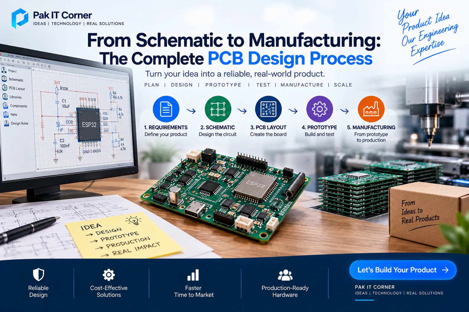
Turning an electronic product idea into a reliable physical circuit board requires much more than simply drawing a schematic. Professional PCB design is a structured engineering process that begins with requirements and continues through schematic design, component selection, PCB layout, manufacturing, assembly, testing, and production validation.
A mistake made during the early stages can lead to failed prototypes, unstable hardware, manufacturing delays, or expensive redesigns. Following a proper PCB design process helps reduce these risks and makes the transition from prototype to production much smoother.
This guide explains the complete PCB design process from the first product idea to manufacturing-ready hardware.
What Is PCB Design?
Printed Circuit Board (PCB) design is the process of converting an electronic circuit concept into a physical board that electrically and mechanically connects all required components.
A complete PCB design normally includes:
- System architecture
- Component selection
- Schematic capture
- Power supply design
- PCB stack-up
- Component placement
- Signal routing
- Ground and power planes
- Design-rule verification
- Manufacturing files
- Assembly documentation
- Prototype testing
- Design revisions
- Production preparation
Good PCB design must consider electrical performance, mechanical requirements, manufacturability, reliability, cost, and future scalability.
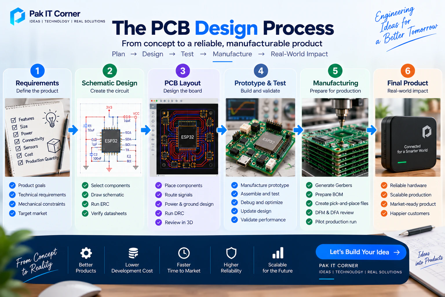
1. Define the Product Requirements
Before opening PCB design software, clearly define what the product needs to do.
Typical requirements include:
- Input voltage
- Output voltages
- Maximum current
- Microcontroller or processor
- Sensors
- Wireless connectivity
- Communication interfaces
- Battery requirements
- Display or user interface
- Motors, relays, pumps, or other loads
- USB connectivity
- Operating temperature
- PCB dimensions
- Mounting requirements
- Environmental conditions
- Expected production quantity
For an IoT product, requirements might include an ESP32 microcontroller, Wi-Fi, Bluetooth, sensors, battery charging, USB-C, status LEDs, and a companion mobile application.
Clear requirements reduce major design changes later.
2. Create the System Block Diagram
A block diagram provides a high-level view of the entire electronic system before individual components are connected.
For example:
Power Input → Protection → Voltage Regulation → Microcontroller
The microcontroller may then connect to:
- Sensors
- Display
- Bluetooth/Wi-Fi
- LoRa
- GNSS/GPS
- Motor drivers
- Relays
- Memory
- USB
- Debug interface
A block diagram makes it easier to understand how different parts of the product interact and helps identify missing interfaces early.
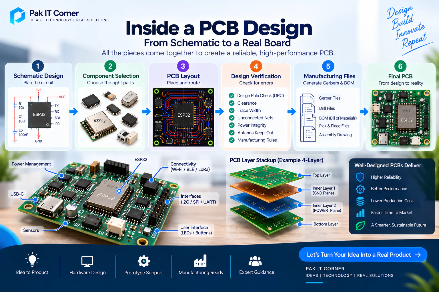
3. Select the Main Components
Once the architecture is defined, the next step is selecting components.
Important considerations include:
- Electrical specifications
- Package size
- Cost
- Availability
- Manufacturer support
- Operating temperature
- Power consumption
- Lifecycle status
- Certification requirements
- Assembly capability
For example, a connected IoT device might use:
- ESP32-S3 for processing and wireless connectivity
- Buck converter for voltage regulation
- Battery charger IC
- USB-C connector
- Environmental sensors
- GNSS module
- LoRa transceiver
- MOSFET drivers
- Protection components
Component selection should always be based on actual system requirements rather than simply choosing familiar parts.
4. Check Component Availability
A technically perfect component is not useful if it cannot be purchased when production begins.
Before finalizing the design, check:
- Current stock
- Supplier availability
- Minimum order quantity
- Lead time
- Alternative components
- Package availability
- Lifecycle status
Where possible, identify alternative parts for components that may become difficult to source.
This becomes especially important when moving from five prototype boards to hundreds or thousands of units. To plan your development and manufacturing budget realistically, see our breakdown of custom PCB design costs in 2026.
5. Study the Datasheets
Datasheets should guide the design.
For every important IC, verify:
- Supply voltage
- Current consumption
- Pin functions
- Absolute maximum ratings
- Recommended operating conditions
- Required capacitors
- Power sequencing
- PCB layout recommendations
- Thermal requirements
- Communication timing
- Reference circuits
Do not assume that two similar components can be connected in exactly the same way.
Manufacturer reference designs are especially useful for switching regulators, RF circuits, USB interfaces, battery chargers, and high-speed electronics.
6. Create the Schematic
The schematic represents the electrical connections between components.
A professional schematic should be organized into logical functional sections such as:
- Power input
- Voltage regulation
- Microcontroller
- Sensors
- Communication
- USB
- Battery management
- Motor or relay control
- Programming/debugging
- User interface
Clear net names and labels make the schematic easier to review and debug.
Instead of drawing long wires across the entire schematic, meaningful labels such as:
SDA, SCL, MOSI, MISO, TX, RX, 3V3, 5V, VBAT
can improve readability significantly.
7. Design the Power Architecture Carefully
Power problems are among the most common causes of prototype failure.
The power architecture should consider:
- Input voltage range
- Peak current
- Average current
- Battery voltage
- Regulator efficiency
- Startup current
- Voltage drops
- Thermal performance
- Noise
- Protection
Different parts of the system may require different voltage rails such as:
12 V → 5 V → 3.3 V
or:
Battery → 3.3 V regulator → MCU and sensors
A wireless microcontroller can draw short current peaks significantly higher than its average current, so regulators must be sized appropriately.
8. Add Decoupling and Bulk Capacitors
Integrated circuits require stable local power.
Decoupling capacitors are normally placed close to IC power pins to provide short bursts of current and reduce high-frequency noise.
Common values include:
- 100 nF ceramic capacitors near IC supply pins
- 1 μF to 10 μF local capacitors
- Larger bulk capacitors near regulators or high-current loads
The correct values should always follow the component datasheet and system requirements.
Good capacitor placement is just as important as choosing the correct value.
9. Add Input and Output Protection
Products operating outside controlled laboratory conditions should include appropriate protection.
Depending on the application, this may include:
- Reverse-polarity protection
- Overvoltage protection
- ESD protection
- TVS diodes
- Input fuses
- Current limiting
- Battery protection
- Flyback diodes
- Surge protection
USB, external connectors, power inputs, sensor cables, and communication interfaces are common locations where protection is important.
10. Run Electrical Rule Checking
Before beginning the PCB layout, run the schematic's Electrical Rule Check (ERC).
ERC can help detect:
- Unconnected pins
- Incorrect power connections
- Output-to-output conflicts
- Missing power flags
- Incomplete nets
However, ERC cannot determine whether the entire engineering design is correct.
A manual schematic review is still essential.
11. Assign PCB Footprints
Every schematic component requires a physical footprint.
Examples include:
- 0402 resistor
- 0603 capacitor
- QFN IC
- SOIC IC
- USB-C connector
- ESP32 module
- JST connector
Footprints must match the exact components that will be purchased.
A footprint error can make an otherwise correct PCB unusable.
Always verify:
- Pad dimensions
- Pin numbering
- Component orientation
- Mechanical dimensions
- Exposed pads
- Connector positioning
12. Define the PCB Shape and Mechanical Constraints
Before component placement, define the physical board.
Consider:
- Board dimensions
- Mounting holes
- Enclosure dimensions
- Connector locations
- Display position
- Buttons
- LEDs
- Antennas
- Sensors
- Cable access
- Keep-out areas
Mechanical constraints should ideally be coordinated with enclosure design early in the project.
Changing connector locations after an enclosure has been manufactured can be expensive.
13. Choose the PCB Layer Stack-Up
Simple designs may use two layers, while more complex products often benefit from four or more layers.
A common four-layer structure is:
- Layer 1 — Signals and components
- Layer 2 — Ground plane
- Layer 3 — Power and signals
- Layer 4 — Signals and components
Four-layer boards can provide better:
- Ground integrity
- EMI performance
- Signal return paths
- Routing flexibility
- Power distribution
The appropriate layer count depends on circuit complexity, signal speed, RF requirements, size, and budget.
14. Place Components Strategically
Component placement strongly affects PCB performance.
Start with major components such as:
- Microcontroller
- Wireless modules
- Connectors
- Power regulators
- Large capacitors
- Sensors
- Displays
- Motor drivers
Then place supporting components around them.
Related components should generally remain close together.
For example, the input and output capacitors of a switching regulator should be positioned according to the manufacturer's recommended layout.
15. Consider Wireless Antenna Placement
Wireless products require special PCB attention.
Wi-Fi, Bluetooth, LoRa, GNSS, and other RF systems can perform poorly if antenna placement is incorrect.
Avoid placing:
- Copper under antenna keep-out areas
- Batteries directly against antennas
- Large metal objects near antennas
- Noisy switching circuits near sensitive RF sections
For modules such as ESP32, follow the manufacturer's antenna keep-out recommendations.
A perfectly functioning circuit can still become a poor product if its wireless range is unreliable.
16. Create a Solid Ground Strategy
Ground is one of the most important parts of PCB design.
A solid ground plane helps:
- Reduce noise
- Improve signal integrity
- Provide return paths
- Improve EMI performance
- Stabilize analog measurements
Avoid unnecessary splits in the ground plane unless there is a specific engineering reason.
High-current return paths should also be considered carefully so they do not interfere with sensitive analog or RF circuits.
17. Route Power Traces Correctly
Power traces must support the expected current.
Trace width depends on:
- Current
- Copper thickness
- Temperature rise
- Trace length
- PCB layer
- Available board space
High-current paths for motors, pumps, LEDs, heaters, or battery systems may require significantly wider traces or copper pours.
Thin traces should not be used for high-current loads simply because they are easier to route.
18. Route Critical Signals First
Critical signals should generally be routed before less important GPIO signals.
Examples include:
- USB
- High-speed clocks
- Differential pairs
- RF signals
- Crystal connections
- Switching regulator loops
- Sensitive analog signals
These signals may require specific routing rules.
19. Route I2C, SPI, and UART Properly
Embedded products commonly use several communication interfaces.
I2C
I2C uses SDA and SCL.
Consider:
- Pull-up resistors
- Bus capacitance
- Voltage compatibility
- Trace length
- Device addresses
SPI
SPI normally uses:
- MOSI
- MISO
- SCLK
- CS
High clock speeds may require careful routing and shorter traces.
UART
UART commonly uses:
- TX
- RX
Always verify that TX from one device connects to RX on the other and vice versa.
20. Design USB-C Correctly
USB-C requires more than simply connecting power pins.
Depending on the application, consider:
- CC resistors
- D+ and D− routing
- ESD protection
- VBUS handling
- Connector shield
- USB data requirements
- USB Power Delivery if required
For USB 2.0 data, D+ and D− should be treated as a differential pair and routed appropriately.
21. Design Switching Regulators Carefully
Buck and boost converters can generate significant electrical noise.
Important layout considerations include:
- Minimize high-current switching loops
- Keep input capacitors close
- Keep output capacitors close
- Keep feedback traces away from switching nodes
- Use suitable ground connections
- Follow the manufacturer's reference layout
For switching regulators, PCB layout is part of the circuit design.
A correct schematic with poor layout can still fail.
22. Separate Sensitive and Noisy Circuits
Sensitive circuits should be protected from noisy sections.
Examples of noisy circuits include:
- Motors
- Relays
- Switching regulators
- High-current LEDs
- RF transmitters
Sensitive circuits include:
- ADC inputs
- Precision sensors
- Analog amplifiers
- GNSS receivers
- Low-level measurement circuits
Placement, grounding, filtering, and routing should be used to reduce interference.
23. Add Test Points
Test points make prototype debugging and production testing much easier.
Useful test points may include:
- Battery voltage
- 5 V
- 3.3 V
- Ground
- Reset
- UART TX/RX
- I2C SDA/SCL
- SPI signals
- Programming pins
- Important analog signals
A few carefully placed test points can save hours during debugging.
24. Include Programming and Debug Interfaces
Embedded products should provide a reliable way to program and debug the microcontroller.
Depending on the MCU, this may include:
- UART
- JTAG
- SWD
- USB
- Tag-Connect
- Pogo-pin test pads
Production programming requirements should be considered during the PCB design rather than after manufacturing.
25. Verify Component Orientation
Orientation errors are common prototype problems.
Carefully verify:
- IC pin 1
- LEDs
- Diodes
- Electrolytic capacitors
- Connectors
- MOSFETs
- Transistors
- Battery connectors
Silkscreen markings should make orientation clear during assembly and inspection.
26. Run Design Rule Checking
Once routing is complete, run the PCB Design Rule Check (DRC).
DRC can detect:
- Clearance violations
- Trace-width violations
- Unconnected nets
- Copper conflicts
- Via issues
- Board-edge violations
Manufacturing capabilities should be reflected in the design rules.
27. Perform a Manual PCB Review
Automated checks are not enough.
Before manufacturing, manually inspect:
- Power routing
- Ground planes
- Antenna areas
- Connector orientation
- Footprints
- Mounting holes
- Silkscreen
- Test points
- Sensitive signals
- High-current paths
- Board dimensions
A second engineer reviewing the design can often identify issues the original designer overlooked.
28. Review the PCB in 3D
Modern PCB design tools provide 3D visualization.
A 3D review helps identify:
- Incorrect connector placement
- Component collisions
- Mechanical interference
- Wrong component height
- Enclosure conflicts
- Orientation issues
3D inspection is particularly useful when the PCB must fit inside a custom enclosure.
29. Generate Manufacturing Files
Once the PCB is approved, manufacturing files can be generated.
Typical deliverables include:
- Gerber files
- Drill files
- Board outline
- Fabrication notes
These files tell the PCB manufacturer how to fabricate the bare board.
Always review the generated Gerbers before sending them for production.
30. Prepare the Bill of Materials
The Bill of Materials (BOM) lists the components required to assemble the board.
A useful BOM may include:
- Reference designator
- Quantity
- Component value
- Manufacturer
- Manufacturer part number
- Supplier part number
- Package
- Description
Accurate manufacturer part numbers reduce purchasing and assembly errors.
31. Generate Pick-and-Place Files
Automated PCB assembly requires component placement information.
The pick-and-place or centroid file normally contains:
- Reference designator
- X coordinate
- Y coordinate
- Rotation
- PCB side
Incorrect rotations or footprints can cause assembly problems, so these files should be reviewed before production.
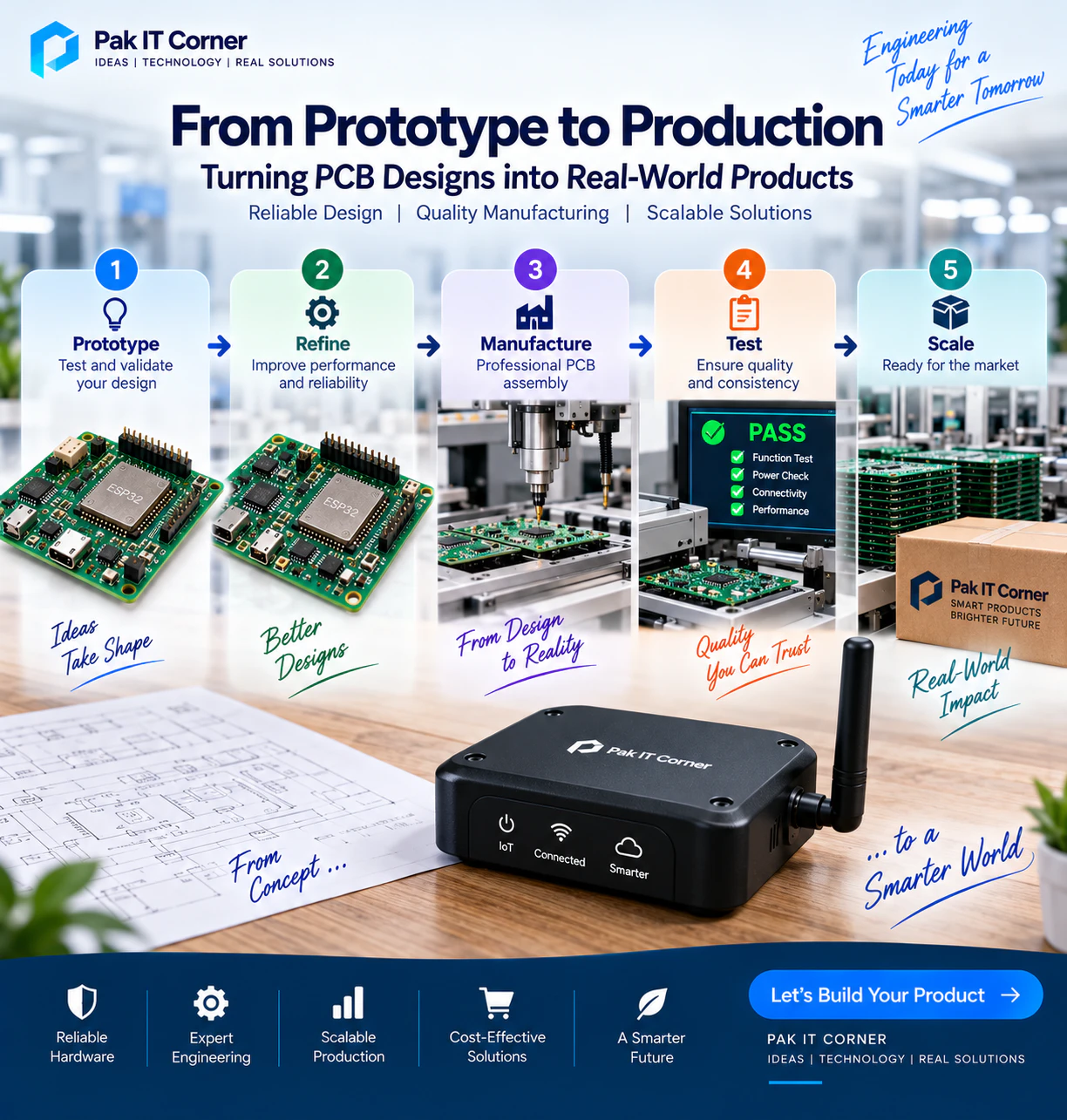
32. Order Prototype PCBs
Do not normally move directly from a new design to large-scale manufacturing.
Start with a small prototype quantity.
The first boards allow engineers to verify:
- Electrical design
- Component footprints
- Mechanical fit
- Wireless performance
- Firmware compatibility
- Thermal behavior
- Power consumption
Prototype quantities depend on the project, but the objective is to discover problems before production quantities increase.
33. Assemble the Prototype
Prototype assembly may be performed:
- Manually
- Using a reflow process
- By a professional PCB assembly service
For complex boards with fine-pitch components, professional assembly is often preferable.
After assembly, visually inspect the board before applying power.
34. Perform the First Power-Up Safely
Do not immediately connect a new board to an unrestricted high-current power source.
A safer first power-up may use a current-limited bench power supply.
Check:
- Input current
- Short circuits
- 3.3 V rail
- 5 V rail
- Other regulated voltages
- Component temperatures
If current suddenly rises beyond expectations, disconnect power and investigate.
35. Test Each Subsystem Individually
Avoid testing the entire product at once.
Test individual sections such as:
- Power supply
- Microcontroller
- USB/programming
- Sensors
- Display
- Bluetooth
- Wi-Fi
- LoRa
- GNSS
- Motors or relays
This approach makes troubleshooting much easier.
36. Bring Up the Firmware
Once basic hardware operation is verified, firmware can be loaded.
Early test firmware should focus on hardware validation rather than full product functionality.
Useful tests include:
- GPIO toggle
- I2C scanner
- SPI communication
- UART communication
- ADC readings
- Sensor detection
- Wi-Fi connection
- Bluetooth advertising
- Battery voltage measurement
Hardware test firmware helps separate PCB problems from application-software problems.
37. Measure Power Consumption
Battery-powered products require detailed power measurements.
Measure:
- Startup current
- Idle current
- Active current
- Wi-Fi transmission current
- Bluetooth current
- Sleep current
- Sensor current
- Peak load current
These measurements can reveal whether the expected battery runtime is realistic.
38. Test Wireless Performance
For connected devices, test:
- Wi-Fi range
- Bluetooth range
- LoRa range where applicable
- GNSS reception
- Reconnection behavior
- Operation near the enclosure
- Performance near the battery
- Interference between radios
Wireless performance should be tested with the actual product enclosure whenever possible.
39. Perform Thermal Testing
Check whether any components become excessively hot.
Pay particular attention to:
- Voltage regulators
- MOSFETs
- Battery chargers
- Motor drivers
- High-current connectors
- Power resistors
Thermal problems may require larger copper areas, different components, improved airflow, or a revised power architecture.
40. Test Failure Conditions
A professional product should not only work under ideal conditions.
Test scenarios such as:
- Battery becoming low
- Wi-Fi disconnecting
- Bluetooth disconnecting
- Sensor failure
- Server unavailable
- Device reset
- Power interruption
- Incorrect user input
- Motor stall
- Overcurrent conditions
The hardware and firmware should recover safely wherever possible.
41. Document Prototype Issues
During testing, maintain a structured list of issues.
For each issue record:
- Problem
- Conditions
- Measurements
- Suspected cause
- Solution
- Required PCB change
- Required firmware change
This information becomes the basis for the next hardware revision.
42. Create the Second PCB Revision
It is normal for professional products to require multiple PCB revisions.
Typical changes may include:
- Different resistor values
- Better filtering
- Improved antenna placement
- Wider traces
- Additional test points
- Connector relocation
- Improved protection
- Component substitutions
- Mechanical adjustments
The objective of the second revision is to resolve issues discovered during real hardware testing.
43. Design for Manufacturing
A prototype that works is not automatically ready for mass production.
Design for Manufacturing (DFM) considers whether the PCB can be produced consistently and economically.
DFM considerations include:
- Standard trace widths
- Standard vias
- Appropriate component spacing
- Common package sizes
- Panelization
- Solder-mask clearance
- Assembly access
- Component availability
Manufacturing partners may provide specific DFM rules.
44. Design for Assembly
Design for Assembly (DFA) focuses on making the board easier and more reliable to assemble.
Consider:
- Consistent component orientation
- Adequate spacing
- Avoiding unnecessary component varieties
- Clear polarity markings
- Accessible connectors
- Suitable footprints
Better assembly design can reduce manufacturing cost and defects.
45. Design for Testing
Production units should be testable quickly.
Design for Test (DFT) may include:
- Pogo-pin pads
- Programming pads
- Power test points
- Communication test points
- Automated test firmware
- Serial-number programming
For larger production quantities, a dedicated test jig can significantly improve manufacturing efficiency.
46. Optimize the BOM for Production
Before mass production, review the BOM again.
Look for:
- Expensive components
- Difficult-to-source components
- Long lead times
- Unnecessary part variations
- Components nearing end of life
- Suitable alternatives
Reducing BOM risk can be as important as reducing BOM cost.
47. Prepare Production Documentation
A manufacturing-ready product should have organized documentation.
This may include:
- Final schematic
- PCB source files
- Gerbers
- Drill files
- BOM
- Pick-and-place files
- Assembly drawings
- Fabrication drawings
- Programming instructions
- Test procedures
- Firmware version
- Mechanical drawings
Good documentation makes future production runs much easier.
48. Run a Pilot Production Batch
Before ordering thousands of units, a smaller pilot batch is often valuable.
A pilot run can reveal:
- Assembly problems
- Component sourcing issues
- Programming problems
- Test-fixture problems
- Mechanical tolerances
- Packaging issues
- Real-world reliability problems
Issues found during a pilot run are much cheaper to correct than problems discovered after mass production.
49. Consider Regulatory Requirements
Depending on the product and target market, certification may be required.
Potential requirements include:
- FCC
- CE
- UKCA
- RoHS
- EMC testing
- Safety testing
- Battery transportation requirements
- Wireless certification
Using pre-certified wireless modules can simplify some parts of the certification process, but it does not automatically make the entire finished product certified.
Regulatory planning should begin early rather than after the product is complete.
50. Move to Mass Production
Once the design has passed prototype testing, pilot production, manufacturing review, and applicable compliance requirements, it can move toward larger production quantities.
Production should maintain:
- Controlled PCB revision
- Controlled BOM revision
- Firmware versioning
- Quality-control procedures
- Programming records
- Test results
- Serial-number tracking where required
Good revision control prevents different hardware versions from becoming mixed during manufacturing.
Common PCB Design Mistakes
Some common mistakes include:
- Selecting components without checking availability
- Incorrect footprints
- Poor power-supply design
- Missing decoupling capacitors
- Inadequate protection
- Thin high-current traces
- Poor ground layout
- Incorrect antenna placement
- Routing under RF antennas
- Missing test points
- Wrong connector orientation
- Ignoring enclosure requirements
- Skipping prototype testing
- Moving directly into large production quantities
Avoiding these mistakes can save significant development time and cost.
PCB Design Software
Popular PCB design tools include:
KiCad
A powerful open-source PCB design platform suitable for many professional projects.
Altium Designer
A widely used professional electronics design platform with advanced PCB development capabilities.
EasyEDA
A convenient PCB design environment with strong integration with component libraries and PCB manufacturing services.
The best tool depends on the project, team, workflow, and manufacturing requirements.
PCB Design for IoT Products
IoT PCB design introduces additional challenges because hardware, firmware, wireless communication, cloud services, and mobile applications must work together.
A typical IoT product may include:
Sensors → Microcontroller → BLE/Wi-Fi/LoRa → Cloud → Mobile App
PCB engineers therefore need to consider:
- Wireless performance
- Battery life
- Device provisioning
- OTA firmware updates
- Security
- Sensor accuracy
- Power consumption
- Enclosure effects
- Mobile-app communication
The PCB is one part of a larger connected ecosystem — explore our guide on how to build an IoT app that connects to hardware.
PCB Design for ESP32 Products
ESP32 is widely used for connected products because many variants provide Wi-Fi, Bluetooth, processing power, and extensive peripherals.
When designing an ESP32 PCB, important considerations include:
- Correct 3.3 V supply
- Peak wireless current
- EN/reset circuit
- Boot configuration
- Programming interface
- Decoupling
- Antenna placement
- Ground layout
- USB interface where required
- Sensor interfaces
- Sleep-current optimization
Using an ESP32 development board is useful for initial prototyping, but production products often move to a custom PCB using an ESP32 module.
Prototype PCB vs Production PCB
A prototype PCB focuses primarily on proving that the system works.
A production PCB must additionally consider:
- Cost
- Reliability
- Manufacturing yield
- Component availability
- Testing
- Certification
- Assembly
- Long-term support
- Supply-chain risk
This is why moving from prototype to production is an engineering phase of its own.
How Long Does PCB Design Take?
PCB development time depends on:
- Circuit complexity
- Number of components
- Layer count
- Wireless requirements
- Mechanical constraints
- Availability of components
- Prototype manufacturing
- Testing
- Number of revisions
A simple board may be designed relatively quickly, while a complex connected product can require multiple design and validation cycles.
Rushing the PCB design process often creates more delays later.
Frequently Asked Questions
What files are required for PCB manufacturing?
PCB manufacturers normally require Gerber and drill files. Assembly services may additionally require a BOM and pick-and-place file.
Should I use a 2-layer or 4-layer PCB?
Simple circuits may work well on two layers. More complex, high-speed, RF, or compact designs often benefit from four or more layers.
Do I need a prototype before mass production?
For a new custom electronic product, prototype testing is strongly recommended before committing to large production quantities.
Can an existing schematic be converted into a PCB?
Yes. The schematic should first be reviewed for electrical correctness, component availability, footprints, power requirements, and manufacturability before PCB layout begins.
Can ESP32 be used in a commercial PCB?
Yes. ESP32 modules and chips are widely used in commercial connected products, provided the overall design follows the relevant technical and regulatory requirements.
What is included in professional PCB design?
Depending on the project, professional PCB design may include schematic capture, component selection, PCB layout, DFM review, manufacturing files, BOM preparation, prototype support, and hardware debugging.
From an Idea to a Manufactured Product
A reliable PCB is the result of many engineering decisions.
The complete process can be summarized as:
Requirements → Architecture → Component Selection → Schematic → PCB Layout → Design Review → Manufacturing Files → Prototype → Testing → Revision → Pilot Production → Mass Production
Each stage reduces a different type of risk.
Skipping stages may save time initially, but problems discovered after manufacturing are usually much more expensive to fix.
PCB Design Services at Pak IT Corner
Pak IT Corner provides PCB design and embedded hardware development services for prototypes and production-oriented electronic products.
Our capabilities include:
- Schematic design
- PCB layout
- ESP32 and STM32 hardware
- IoT electronics and companion applications
- Sensor integration
- Wi-Fi, Bluetooth, LoRa, and GNSS integration
- Battery-powered electronics
- Power-supply design
- USB-C integration
- Motor and relay control
- BOM preparation
- Gerber and manufacturing files
- Prototype bring-up
- Firmware integration
- Hardware debugging
- Design-for-manufacturing support
Whether you are developing an early prototype or preparing an existing electronic product for manufacturing, a structured PCB development process can reduce risk and create a stronger foundation for production — view past hardware in our portfolio.
Ready to Develop Your PCB?
If you have an electronics product idea, existing schematic, prototype, or PCB that needs improvement, Pak IT Corner can help take it from circuit design through manufacturing-ready hardware.
Start with clear requirements, validate every engineering stage, and build the product for production — not just for the first prototype.